Interview background: Zhejiang Raysea Technology Co., Ltd. (hereinafter referred to as “Raysea Technology”) was established in 2017 by top VCSEL technical experts who once worked for the Fortune 500. The founding team includes the person in charge of the VCSEL wafer factory of the Fortune 500 and the technical director of the Global Supply Chain Technology and Quality Department of the Fortune 500; The core members are from the VCSEL chip team of the Fortune 500. At present, Raysea Technology has obtained the strategic angel round investment provided by Sunny Industry V Fund in September 2017, and the Pre-A round investment provided by Dachen and Tianchuang in August 2018. The two rounds of financing totaled 100 million yuan and will be mainly used for the mass production of VCSEL chips.
Raysea Technology benchmarking international first-class manufacturers Lumentum and Broadcom (Avago), taking China as the target market and looking globally. This VCSEL enterprise team, which was founded less than a year ago, has a strong presence, backed by the strategic cooperation and support of Sunny Group, and stands in the strong 3D vision industry. It can be said that it has all the advantages of “time, location, and people”! Maims Consulting is honored to interview James Liu, CEO of Raysea Technology. Here are our highlights.
MEMS:First of all, please talk about what prompted you to return to China for entrepreneurship?
James Liu:The core members of Raysea Technology have been engaged in the R&D and production of VCSEL in the industry for more than 20 years, and have witnessed and participated in the whole development process of VCSEL from low speed to high speed, as well as the penetration from the data communication field to the consumer electronics and vehicle mounted laser radar field. As the most versatile laser diode, VCSEL’s huge application potential is emerging in the market. China has the largest optical communication market in the world. Huawei, ZTE, Fenghuo Communication and other world-renowned enterprises have emerged, accounting for more than 40% of the global market share in total. However, most of the optical devices they use depend on imports. With the rapid development of data center and cloud computing, data communication will be the focus of China’s market development, and reliable VCSEL chip supply will become a key link.
At the same time, with the current transformation of optical imaging technology from two-dimensional to three-dimensional, the 3D vision industry is developing rapidly, and the importance of VCSEL is increasingly prominent. However, for a long time, the core technology of VCSEL has been controlled by a few international manufacturers. Only Broadcom (Avago), Sumitomo Electric, Finisar and Lumentum have realized the commercial mass production of high-end products. There has been no mass production of VCSEL products with high yield and high reliability in China. Relying on the leading technology accumulation, Ruixi Technology hopes to help China’s 3D vision industry and data communication industry complete the integration of the value chain from chip to module, and then to the system industry, making contributions to the localization of high-end core chips in key industries!
MEMS:How about the current operation and progress of the company? It is reported that you have made layout in the United States, Hangzhou and other places. What are the priorities of each place?
James Liu:Based on the strategy of global competition and customer service, the company has set up branches in major customers around the world. Headquartered in Yuyao City, Zhejiang Province, it has set up wholly-owned subsidiaries in the United States and Hangzhou, and a support center in Taiwan. Yuyao headquarters is mainly responsible for the company’s administration, personnel and product quality control; The Hangzhou subsidiary is mainly the market and engineering center, which is responsible for market development, maintenance and later technical support; The US R&D Center is mainly responsible for product development and testing and verification of some samples; The Taiwan Branch is mainly responsible for supporting mass production of products and improvement of production process.
Raysea Technology’s wholly-owned subsidiary in Hangzhou
MEMS:VCSEL is a laser that requires high technical threshold and industrial experience. What technical barriers does VCSEL have in design, manufacturing, packaging and reliability verification? Can you give some examples to let us intuitively feel VCSEL’s “unattainable” and how the powerful Raysea Technology has conquered this “peak” of technology.
James Liu:VCSEL integrates disciplines such as semiconductor materials, laser physics, semiconductor manufacturing technology, high-speed RF electronics and optical technology. Not only is the chip complex in structure, but also gallium arsenide materials that are two orders of magnitude more fragile than silicon materials and have higher intrinsic defects are required to meet the requirements of high performance and reliability. During the preparation of VCSEL, the probability of crystal defects caused by stress and manufacturing process is much higher than that of silicon based optoelectronic chips. In addition, when the VCSEL chip is working, the current density per unit volume is much higher than that of the silicon based optoelectronic chip, which means that the VCSEL will bear greater light intensity and current. For example, if the VCSEL design or process is not “perfect” enough, resulting in local crystal defects, it is difficult to detect them in the conventional delivery test; However, in the process of chip operation, crystal defects will accelerate growth under the stimulation of high temperature, high current and strong photons. After a period of time, once the crack growth exceeds a certain value or reaches the active region, the chip will fail.
Compared with silicon based electrical chips, VCSEL chips are closer to the category of material science. Excellent chip design needs to meet high performance indicators, but the biggest challenge is the requirement of high reliability. This involves the optimization of active layer materials, structural stress, structural heat dissipation, etc. related to materials and structures, and also depends on the optimization of epitaxial growth and key manufacturing processes. Mature VCSEL products require years of accumulation and countless error correction experiments in terms of reliability process. The mass industrialization of low cost, high performance, high yield and high reliability requires practitioners to have a deep academic theoretical foundation, and more rely on the rich experience accumulated by the industry for many years and the ability to quickly solve problems.
With the craftsmanship spirit of 20 years, the core members of Raysea Technology have been leading the product design and production in the world-class VCSEL company for a long time; Experience covers all fields from chip design, epitaxial growth, process to high-frequency packaging test; Be good at using big data and failure analysis to optimize VCSEL design and batch manufacturing process; The team members have extensive recognition and good reputation in the industry. The development of the company from its establishment to today has also verified our strength
。
MEMS:At present, the main application fields of VCSEL are consumer electronics, data communication and industry. In the future, lidar will become its emerging field. What are the main areas of Raysea Technology? Please explain why you chose these areas.
James Liu:In terms of market, VCSEL currently has two main application scenarios: optical communication system and 3D imaging module. In addition, the application of VCSEL in laser radar and vehicle is also emerging. Although the background of Raysea Technology team is in the field of optical communication, we chose to start from the 3D imaging module of consumer electronics products in the early stage. Our team analyzed that the time window left for VCSEL manufacturers in the mobile phone 3D imaging module market is limited, and the industry may ship in large quantities next year, which is a very good breakthrough in this direction; In addition, the industrial chain of the optical communication industry is relatively stable and closed, and the certification cycle is relatively long, which takes 1 to 1.5 years.
MEMS:What product series has Raysea Technology developed? When is it expected to enter mass production status?
James Liu:At present, the company has completed the third generation VCSEL chip applicable to mobile phones and other consumer electronics. It will be mass produced in 2018, reaching the level of international mainstream manufacturers, and become the only domestic VCSEL chip recommended by Sunny Optics. At this stage, it is negotiating with mobile phone manufacturers about cooperation intentions. At the same time, the team is also developing 4 × 25Gbps (100Gbps) VCSEL chip, 25G high-speed VCSEL and PD have launched high-performance samples in 2018 and are preparing for mass production. It is estimated that sample delivery and mass production will be achieved in 2019. Now the company is also in contact with Hisense, Xuchuang, Ali and other manufacturers.

Developed product series of Raysea Technology
MEMS:Raysea technology team also has a deep technical accumulation in the field of lidar. At present, EEL (edge emitting laser) is the main laser used in lidar. Please introduce the advantages and disadvantages between VCSEL and EEL and their application scope.
James Liu:The vehicle mounted laser radar needs a long enough detection distance, which requires high laser power. EEL (edge emitting laser) has certain advantages over power. At the same time, VCSEL technology is not yet mature in the 1500nm long infrared band, which is safer for human eyes. However, as a solid state laser, VCSEL array does not need scanning mechanical structure, which is not only highly reliable, but also a very promising low-cost solution. It has the potential to reduce the price of vehicle mounted laser radar from nearly ten thousand dollars to several hundred dollars, thereby promoting the popularity of laser radar in the vehicle field. With the development of high power VCSEL and the maturity of high sensitivity receivers in corresponding bands, vehicle mounted lidar using VCSEL has become a research and development hotspot in the industry.
MEMS:As far as we know, VCSEL in the data communication industry often uses a 3-inch or 4-inch wafer manufacturing process, but the consumer electronics industry needs a 6-inch wafer manufacturing process to reduce costs and achieve larger VCSEL arrays. This evolution has a direct impact on the yield of manufacturing. At present, the yield of the 6-inch manufacturing process is still low. Please share your experience on yield control of 6-inch VCSEL manufacturing process based on your previous and recent development experience in Ruixi Technology!
James Liu:Whether it is the traditional 3-inch or 4-inch VCSEL wafer manufacturing process, or the 6-inch VCSEL wafer manufacturing process that is becoming the mainstream at present, maintaining a high manufacturing yield is a challenge to the industry. The 6-inch VCSEL wafer manufacturing process is more challenging, and its key core processes need years of accumulation. The core member of Ruixi Technology, the leading 6-inch wafer manufacturer in the industry, has been running in for more than two years and has established a close partnership. Through the evaluation of the entire industry chain, the team selected two manufacturers with high-quality production capacity for the back-end manufacturing process, whose VCSEL chip manufacturing process accounts for more than 70% of the current total market capacity. At present, Raysea Technology has made more than 100 rounds of streaming in two manufacturers. At the same time, it has developed and implemented new designs and processes for key performance indicators of 3D imaging chips, including power conversion efficiency (PCE) and luminous uniformity. The overall yield has reached a very high level.
MEMS:Raysea Technology directly benchmarking Lumentum, Broadcom (Avago) and other world-class VCSEL enterprises. What are the main sources of confidence? Or what are your competitive advantages compared with international giants?
James Liu:After mass production, the competition between Ruixi Technology and these manufacturers is inevitable. Raysea Technology’s confidence comes from the craftsmanship spirit that the team has accumulated in the VCSEL industry for decades. Relying on the profound technical accumulation, Raysea has completed the development of three generations of products in less than a year since its establishment, and its performance level is no less than that of international mainstream manufacturers. For example, the average power conversion efficiency (PCE) of all chips on the whole 6-inch wafer of the latest generation of 3D structured light VCSEL has reached 46%.In terms of chip performance and mass production capacity, it has been at the leading level in the global industry.
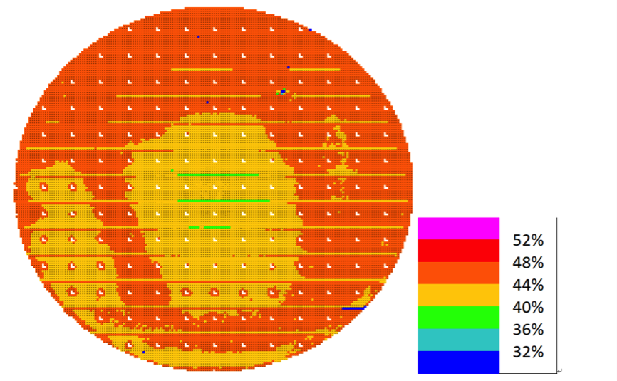
PCE distribution on the latest generation 3D structured light VCSEL 6-inch wafer of Raysea Technology
On the basis of comprehensively catching up with and surpassing the international first-class VCSEL enterprises in product performance and completing the layout of mass production capacity, Raysea Technology, relying on decades of experience in the field of digital communications, is focusing on strengthening the construction of the company’s quality control and establishing its own quality reputation.
From the perspective of industrial development, VCSEL, like LED 20 years ago, is undergoing a process of transfer from Europe and the United States to Asia, especially China, driven by the market. Recognizing this opportunity, Raysea Technology has been determined to take root in the Chinese market since its establishment, provide all-round technical support and services for local customers, and win customer trust. At the same time, relying on the improvement of yield, Raysea Technology will control the cost of chips within a very competitive price range.
In the above aspects, especially product performance and quality control, Raysea Technology will establish its core competitiveness and lay a foundation for the company’s long-term stable development.
MEMS:Lumentum and Broadcom (Avago) both use the IDM mode, while Raysea Technology currently uses the Fabless mode. Do you have any plans to establish VCSEL extension lines or semiconductor process lines? If not, how do you manage the supply chain to ensure stable supply? If so, please talk about the plan.
James Liu:Raysea Technology has thoroughly evaluated these two models. Relying on the current situation that we have enough industrial resources and the reality that VCSEL suppliers using IDM model are facing new challenges, there is no plan and urgency to establish VCSEL extension lines or semiconductor process lines in the short term.
MEMS:Raysea Technology has obtained the strategic angel round investment of Sunny Industry V Fund. Can you disclose the amount and purpose of this round of investment? In addition to capital, do you have any other purpose in choosing Sunny Industry V Fund? For example, we can better cooperate with Sunny Optics.
James Liu:Raysea Technology has obtained the strategic angel round investment provided by Sunny Industry V Fund in September 2017, and the Pre-A round investment provided by Dachen and Tianchuang in August 2018. The two rounds of financing totaled 100 million yuan and will be mainly used for the mass production of VCSEL chips. As the industry leader of camera modules, Sunny Optics provides a very good platform for the evaluation and certification of Ruixi Technology’s VCSEL products.
MEMS:As a strategic partner of Sunny Optical 3D structured light, Raysea Technology has obtained a “shortcut” to provide VCSEL for mobile phone 3D cameras. Can you talk about the current cooperation with domestic first-line mobile phone manufacturers?
James Liu:As the industry leader of camera modules, Sunny Optics provides a very good platform for the evaluation and certification of Raysea Technology’s VCSEL products. At the same time, it also puts forward higher requirements for the development speed and ability of Ruixi Technology. From product performance to the company’s operational capability, we need to compete with the world’s leading manufacturers in the market as soon as possible to win the recognition of customers with our strength.
With the smooth progress of product research and development, Raysea Technology has always maintained active cooperation with first-line mobile phone manufacturers at home and abroad since its establishment.
MEMS:Generally, the VCSEL in the 3D structured light scheme needs to be customized according to customer needs, while the VCSEL in the time of flight (ToF) scheme does not need to be customized, and it has been seen that both Apple and Android are deploying this technology. From the perspective of VCSEL development, is there any difference in the difficulty of VCSEL between the 3D structured light scheme and the ToF scheme? Does Ruixi Technology plan or have been developing VCSEL of ToF scheme?
James Liu:VCSEL in 3D structured light scheme and ToF scheme has different design and process challenges due to different index requirements, so it cannot be evaluated simply by the degree of difficulty. In addition to the 3D structured light chips with leading performance in the industry, Raysea Technology has developed VCSEL chips with different powers for the ToF scheme, which have excellent performance and fully meet the specification requirements of front-line customers.
MEMS:Please look forward to the future goals and corporate vision of Raysea Technology, thank you!
James Liu:In the future, Raysea Technology will take consumer electronic products as a breakthrough; Take high-quality chips as the core competitiveness to strengthen the field of data communication; And vigorously develop the application of VCSEL derivative products in emerging markets. We look forward to embracing the market wave set off by 3D imaging technology, meeting the huge market opportunities brought by 5G optical communication, and becoming the world’s leading VCSEL product supplier!
MEMS:On September 10, Raysea Technology will hold the “24th” Meaningful Words “Seminar: 3D Vision Technology and Application” in Shanghai to promote and display the company to China’s 3D vision industry chain for the first time. You are very much looking forward to the speech of Raysea Technology. What content will you bring to the meeting?
James Liu:The company attaches great importance to this speech and carefully prepares the content of the speech. VCSEL is the next generation mainstream light source, which has the advantages of low power consumption, low cost and high efficiency. It is replacing LD and LED, and is the strategic core element of the “future AI world”. The content of this speech will discuss with the guests the experience of VCSEL technology development, share the progress of Raysea Technology in VCSEL’s industrialization in China, and hope to have full communication with relevant industry experts.
